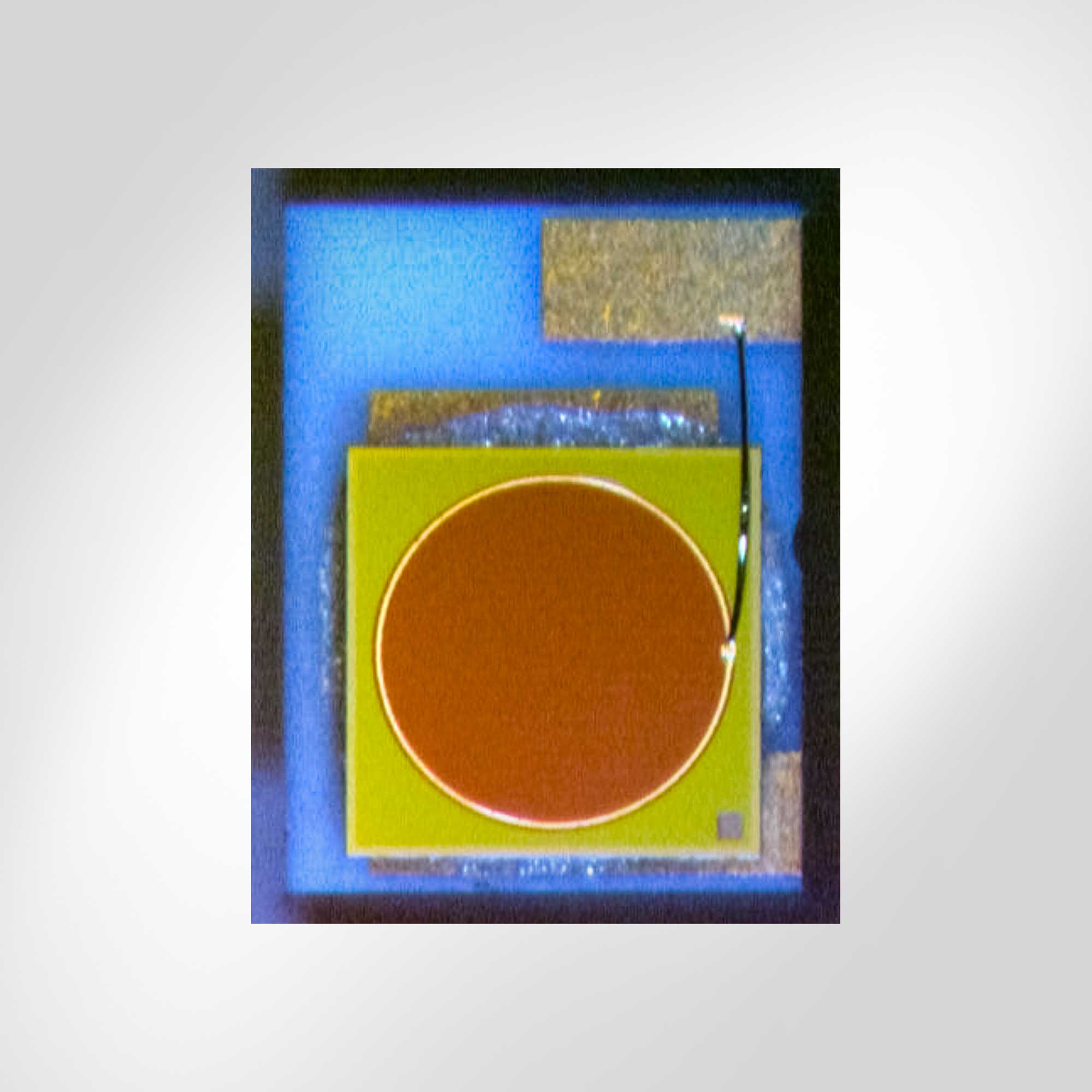
InGaAs Avalanche Photodiode (APD) 2.5 Gbps Chip Front Illuminated GPON / GEPON
Go!Foton PDAF0055C Series are InGaAs APD chip. It is front illuminated type and planer structure with 55 um active area diameter. It is suitable for 2.5 Gbps application in G-PON / GE-PON. APD chip is fabricated at Go!Foton proprietary wafer fab.
- Planer Structure for High Reliability
- 1000 to 1625nm Spectral Response
- Low Dark Current

InGaAs PIN Photodiode With Large Photosensitive Area Chip-On-Carrier
Go!Foton large area Indium Gallium Arsenide (InGaAs) Photodiode consists of pin structure and photo sensitive area of 1 mm diameter with planer structure for high reliability. This PD has photo response in the near infrared spectrum range, between 950 and 1650 nm. This device has very high sensitivity and low noise, making it suitable for industrial application. The photodiode is mounted on ceramic subcarrier. PD chip is fabricated at Go!Foton proprietary wafer fab.
- 950 to 1625nm Spectral Response
- High Sensitivity
- Planer Structure for High Reliability
- High Shunt Resistance
- Low Dark Current
- Low Capacitance
- Chip-on-Carrier

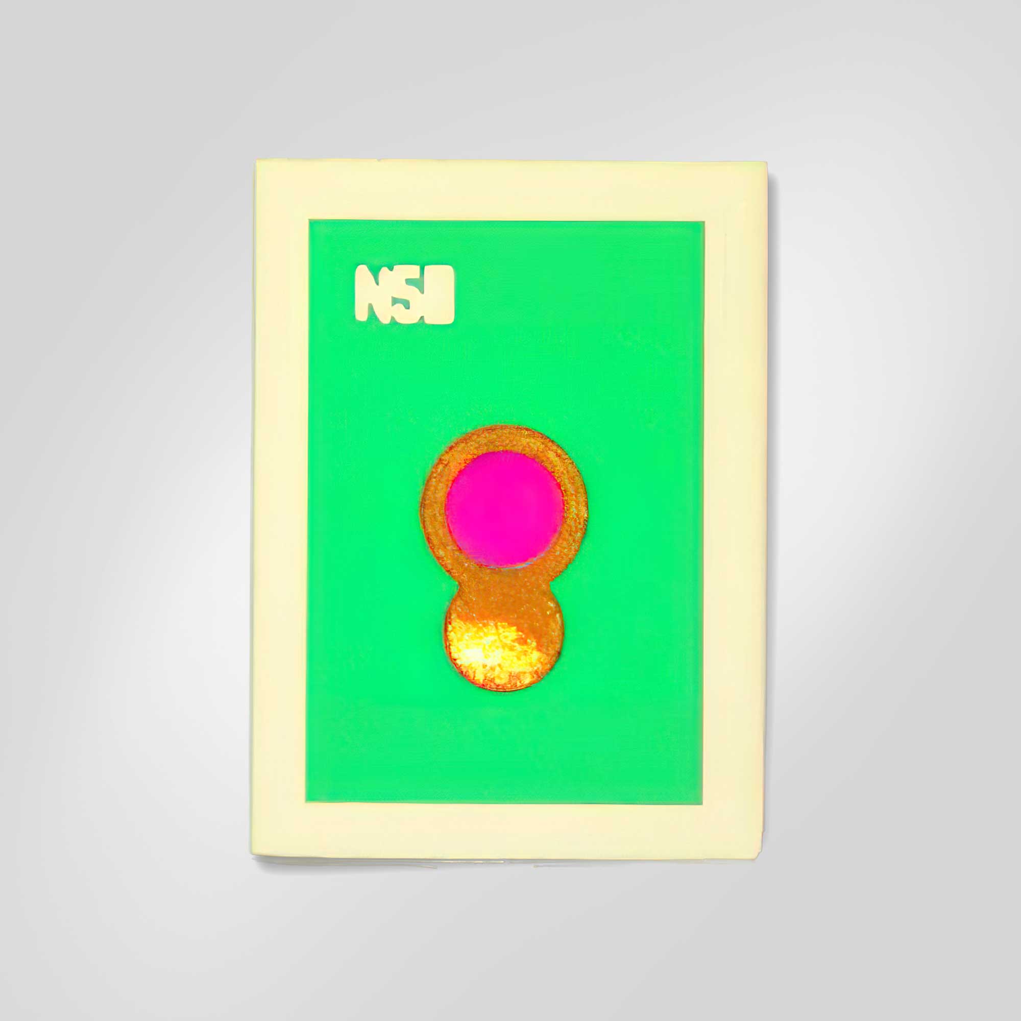
InGaAs PIN Photodiode With Large Photosensitive Area Chip
Go!Foton large area Indium Gallium Arsenide (InGaAs) Photodiode consists of pin structure and photo sensitive area of 1 mm diameter with planer structure for high reliability. This PD has photo response in the near infrared spectrum range, between 950 and 1650 nm. This device has very high sensitivity and low noise, making it suitable for industrial applications. PD chips are fabricated at Go!Foton’s proprietary wafer fab.
- 950 to 1625nm Spectral Response
- Planer Structure for High Reliability
- Low Dark Current
- High Shunt Resistance
- High Sensitivity
- Low Capacitance


